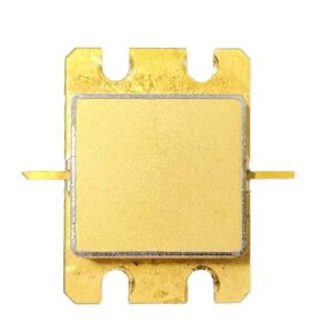
Our capabilities of GaAs/GaN/Si microwave chip
- GaAs/GaN/Si microwave chip
- Comprehensive range, more than 20 categories and more than 500 models
- Domestic substitution, more than 900 models, performance substitution, price 5-60% less than Marki’s Mixer, Hittite’s LNA, VCO, MACOM’s PIN switch, etc.
- Broadband chip with superior performance
- Broadband amplifiers, VCOs, mixers, switching filter banks, etc.
- TR multi-function chip set (S/C/X/Ku/Ka, GaAs/GaN transceiver + GaAs/Si amplitude and phase)
- Customized multi-function chip
- Transceiver/amplitude-phase multi-function, bidirectional amplifier, switching filter bank, mixing multi-function, power dividing network, etc.
- Packaging devices (plastic packaging, low-cost ceramic and gold packaging, SIP)
Our key products
- Broadband low noise amplifier
- Low Phase Noise, Low Noise Amplifier
- Gallium Arsenide Power Amplifier
- GaN power amplifier
- Broadband MIXER
- Wideband limiter
- High Power FET Switch
- Low cost device
- Gallium arsenide multi-function chip
- Silicon based products
- SIP surface mount multi-function device
- Surface mount power amplifier
- Internally matched amplifier
- Ceramic filter
- Low-cost, high-reliability ceramic-metal sealing device
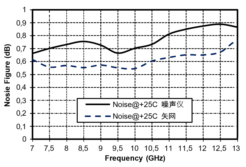
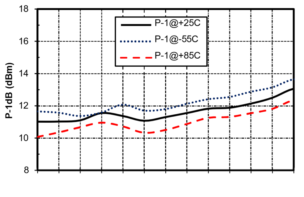
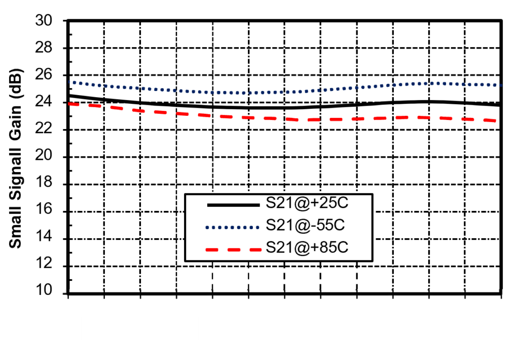
New product 7~13G broadband ultra-low noise LNA
Features:
- Frequency range: 7-13GHz
- Small signal gain: 23.5dB
- Gain flatness: ±0.5dB
- Noise figure: 0.6dB typ. (Yanet test)
- P-1dB: 11.5dBm
- Power supply: +5V/40mA
6~18G broadband universal LNA
Features:
- Frequency range: 6-18GHz
- Small signal gain: 24dB (positive slope)
- Gain flatness: ±1.3dB
- Noise figure: 1.3dB Max.; 1.0dB Typ.
- P-1dB: 13.5dBm
- Power supply: +5V/35mA
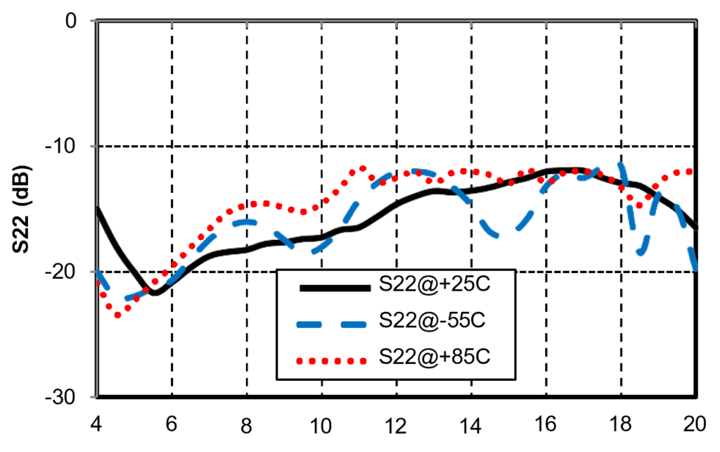
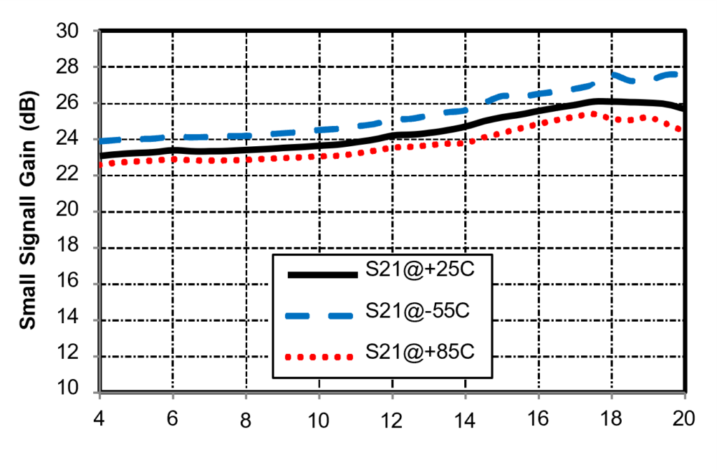
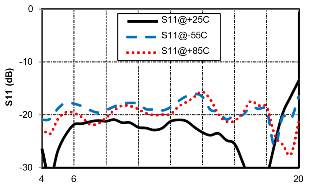
test curve
0.5~20G ultra-wideband high-gain LNA
Features:
- Frequency range: 0.5-20GHz
- Small signal gain: 27.5dB
- Gain Flatness: ±1.0
- Noise figure: 2.0dB
- P-1dB: 15.5dBm
- Power supply: +5V/65mA (static)

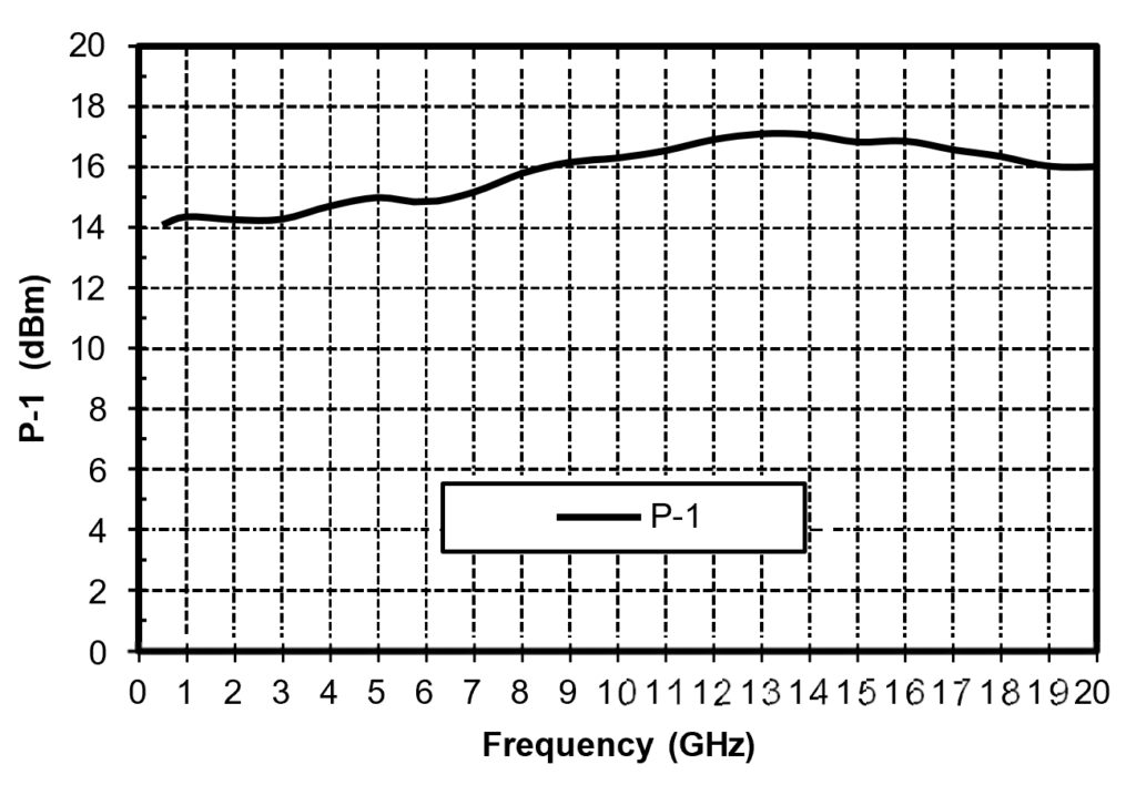
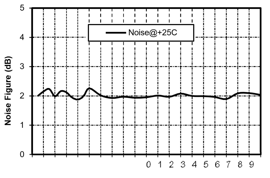
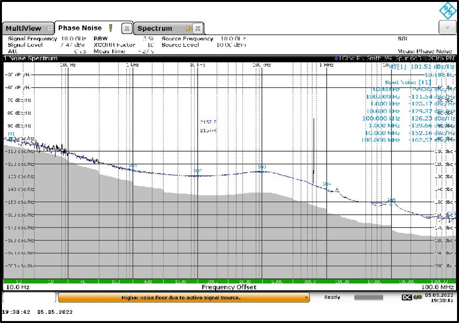
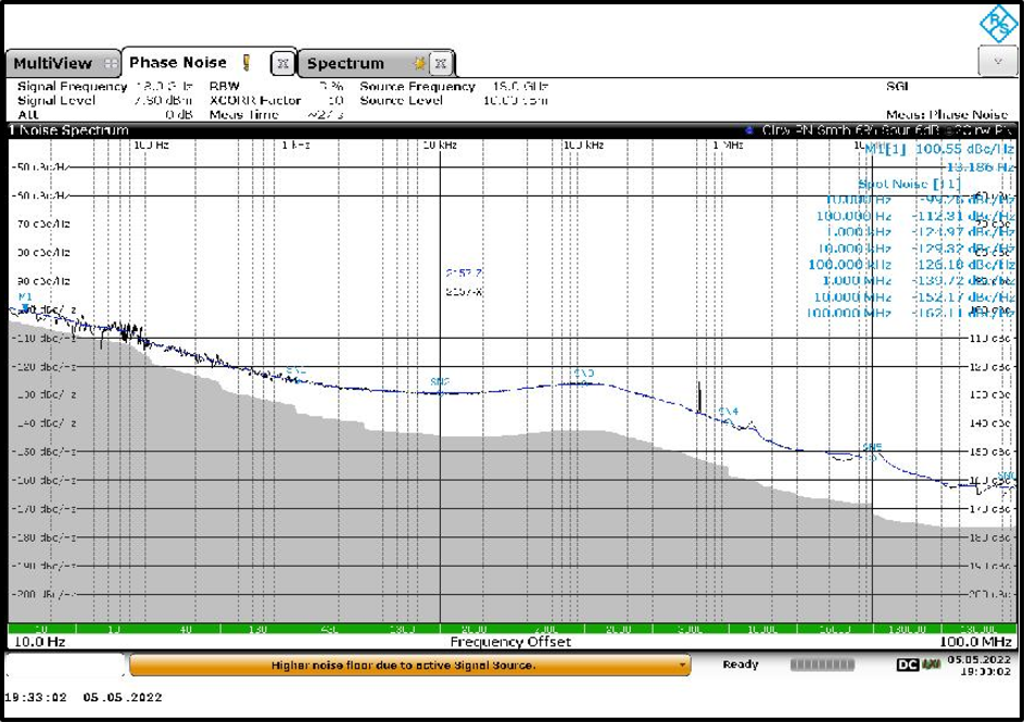
Low phase noise amplifier
Features:
- Frequency coverage: 0.01~18G
- Considering the characteristics of low phase noise and low noise
- Can achieve foreign low phase noise PIN-PIN compatibility and core index compatibility with NBB400, HMC606, HMC3653, HMC3587
| Frequency Range(GHz) | Gain(d B) | noise coefficient( dB) | phase noise(dBc/Hz) | P-1dB (dBm) | input Output Return loss(dB) | Benchmark model |
| 0.01-3.5 | 26 | 13 | -175@1MHz offset@100MHz | 20 | 10/10 | NBB400 |
| DC-4 | 20.5 | 3.5 | -175@1MHz offset@100MHz | 13.5 | 15/15 | NBB400 |
| 2-18 | 13.5 | 4.7 | 112@100Hz@18GHz,124@1KHz@18GHz 126@10KHz@18GHz,139@1MHz@18GHz | 15.5 | 10/10 | HMC606 |
| 4-16 | 14.5 | 4.0 | 145@100Hz@10GHz,155@1KHz@10GHz 160@10KHz@10GHz,165@1MHz@10GHz | 13.5 | 10/10 | HMC3653 |
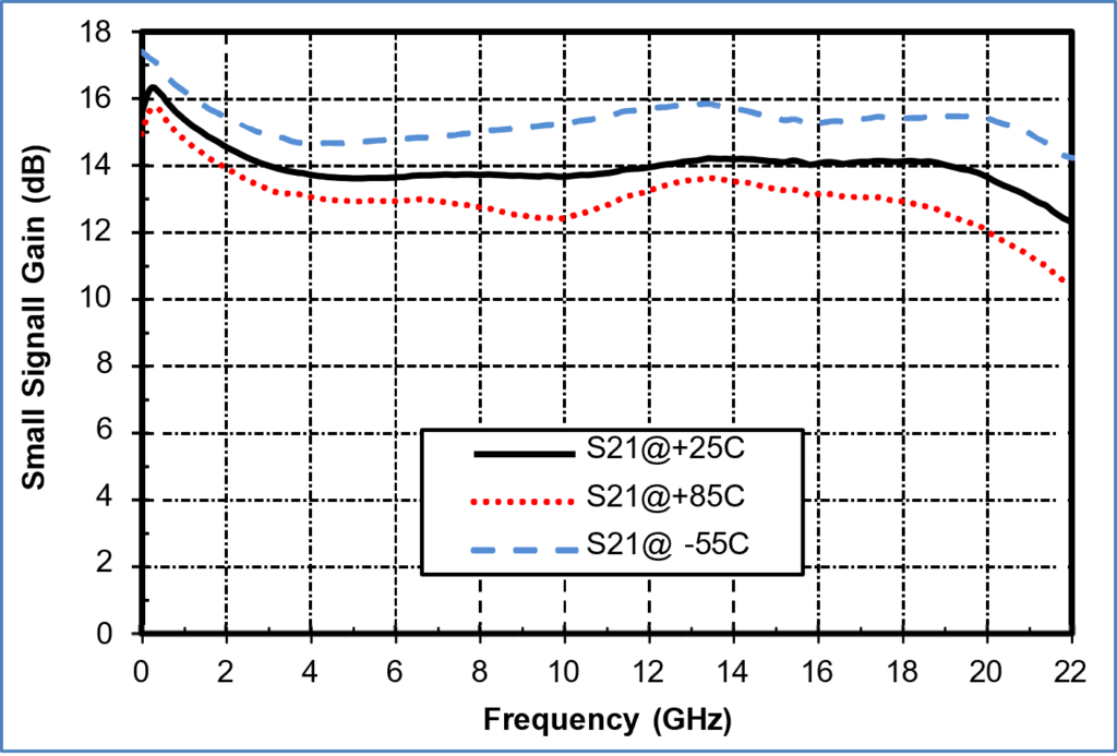
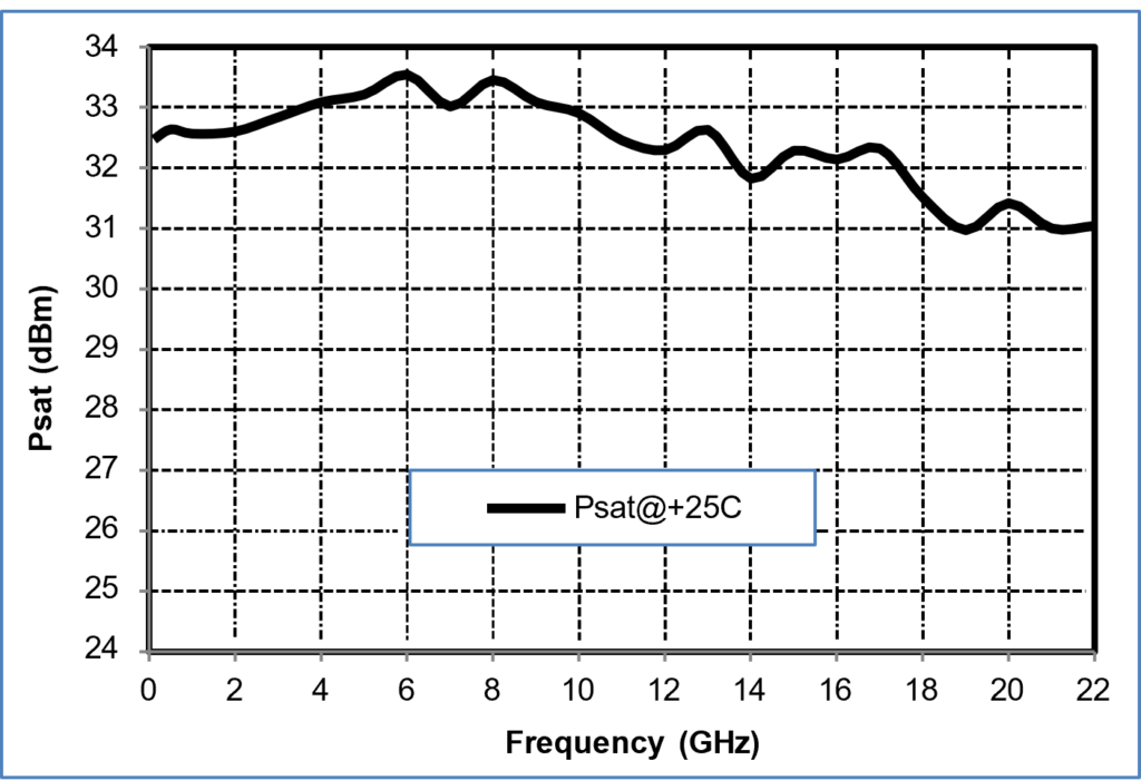
Gallium Arsenide Power Amplifier DC~22G ultra-wideband power amplifier
Features:
- Frequency range: DC-22GHz
- Small signal gain: 13.5dB
- Psat: 32dBm
- Power supply: +15V@480mA
- Replaces HMC998A
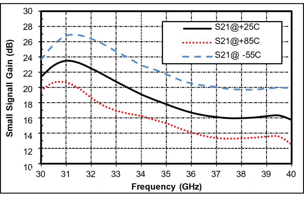
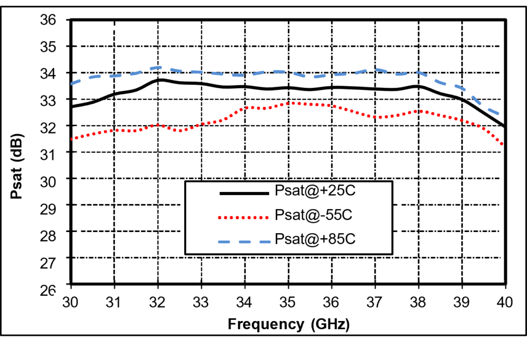
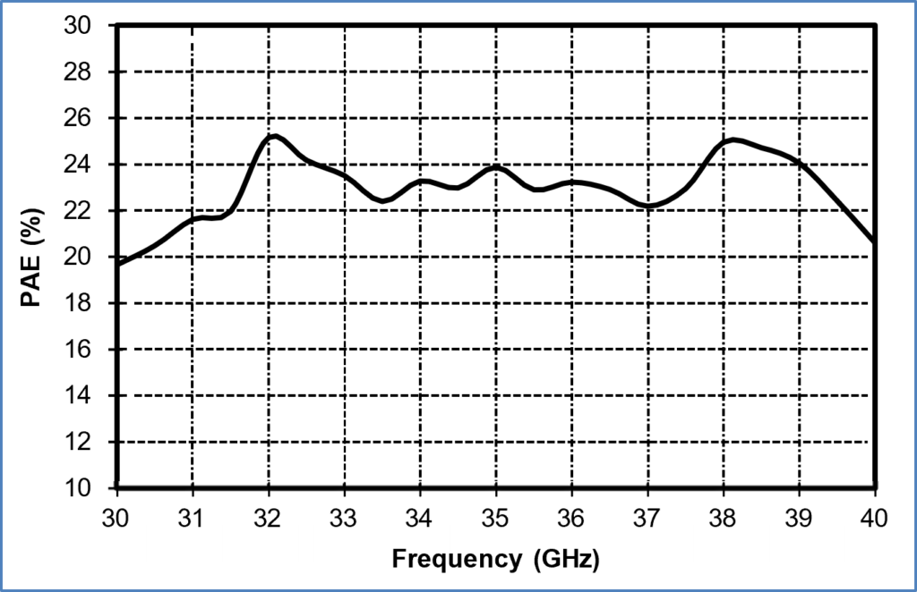
32~38G broadband power amplifier
Features:
- Frequency range: 32-38GHz
- Small signal gain: 18dB
- Psat: 33.5dBm
- Power supply: +6V@1200mA, 1500mA under RF drive
- Replaces TGA4516
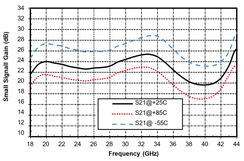
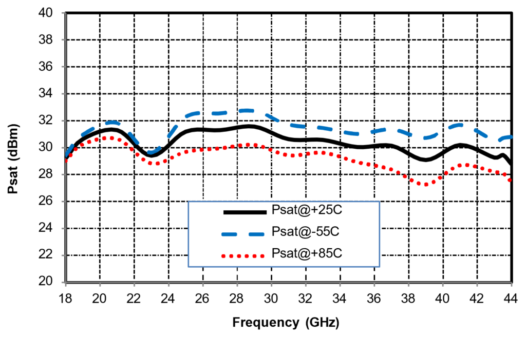
18~44G broadband power amplifier
Features:
- Frequency range: 18-44GHz
- Small signal gain: 22.5dB
- Psat: 30dBm
- Power supply: +5V@1350mA
- Replaces ADPA7007
GaN MMIC power amplifiers
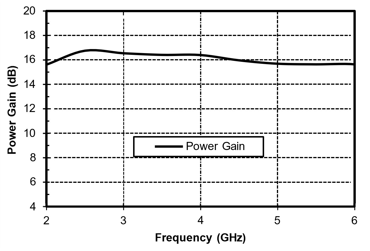
| Frequency Range(GHz) | power gain(dB) | power gain flatness(dB) | Psat (dBm) | PAE (%) | Input return loss(dB) | Operating mode |
| 0.3-6.5 | 13.5 | ±1.1 | 34 | 20 | 15 | CW |
| 0.3-2.5 | 25 | ±1.65 | 41 | 48 | 15 | CW |
| 1-4 | 11 | ±1.0 | 46 | 27 | 19 | CW |
| 1-8 | 17 | ±2.0 | 40 | 30 | 17 | CW |
| 2-6 | 19 | ±1.2 | 34 | 43 | 19 | CW |
| 2-6 | 15 | ±1.5 | 46 | 33 | 12 | CW |
| 8-12 | 15 | ±0.6 | 43 | 34 | 22 | CW |
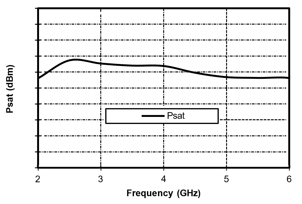
Featured GaN MMIC Products
LNPA2735-50-130
50-130W, 2.7 — 3.5GHz, GaN MMIC, Power Amplifier
LNPA2731-50-130 is a gallium nitride high electronmobility transistor (GaN HEMT). It is a high-power internally matched power transistor that can operate inpulse mode at saturated power and is used in standard communication and radar frequency bands. Provides optimal power and gain performance in 50Ω systems.
Features:
• Coverable working frequency band range: 2.7~3.5GHz;
• Good 50Ω impedance matching, easy to use in cascade;
• Metal ceramic shell sealed package;
• Available in screw-on flange package or welded pill package;
Limit parameters:
• Source-drain voltage Vds: +120V;
• Gate-source voltage Vgs: -10V;
• Dissipated power (Tc=25℃): 110W;
• Storage temperature: -55℃~+125℃;
• Operating temperature: -40℃~+75℃;
LNPA2530-150
150W, 2.5 — 3.0GHz, GaN MMIC, Power Amplifier.
LNPA2530-150 is a gallium nitride high electronmobility transistor (GaN HEMT). It is a high-power internally matched power transistor that can operate inpulse mode at saturated power and is used in standard communication and radar frequency bands. Provides optimal power and gain performance in 50Ω systems.
Features:
•Coverable working frequency band range: 2.55~3.0GHz;
• Good 50Ω impedance matching, easy to use in cascade;
• Metal ceramic shell sealed package;
• Available in screw-on flange package or welded pill package;
Limit parameters:
• Source-drain voltage Vds: +100V;
• Gate-source voltage Vgs: -10V;
• Dissipated power (Tc=25℃): 89W;
• Storage temperature: -55℃~+125℃;
• Operating temperature: -40℃~+75℃;
LNPA2731-150-260
150-260W, 2.7 — 2.9 GHz, GaN MMIC, Power Amplifier
LNPA2731-150-260 is a gallium nitride high electronmobility transistor (GaN HEMT). It is a high-power internally matched power transistor that can operate inpulse mode at saturated power and is used in standard communication and radar frequency bands. Provides optimal power and gain performance in 50Ω systems.
Features:
• Coverable working frequency band range: 2.7~2.9GHz;
• Good 50Ω impedance matching, easy to use in cascade;
• Metal ceramic shell sealed package;
• Available in screw-on flange package or welded pill package;
Limit parameters:
• Source-drain voltage Vds: +120V;
• Gate-source voltage Vgs: -10V;
• Dissipated power (Tc=25℃): 94W;
• Storage temperature: -55℃~+125℃;
• Operating temperature: -40℃~+75℃;
LNPA2731-350
350W, 2.7 — 3.1 GHz, GaN MMIC, Power Amplifier
LNPA2731-350 is a gallium nitride high electronmobility transistor (GaN HEMT). It is a high-power internally matched power transistor that can operate inpulse mode at saturated power and is used in standard communication and radar frequency bands. Provides optimal power and gain performance in 50Ω systems.
Features:
• Coverable working frequency band range: 2.7~3.1GHz;
• Good 50Ω impedance matching, easy to use in cascade;
• Metal ceramic shell sealed package;
• Available in screw-on flange package or welded pill package;
Limit parameters:
• Source-drain voltage Vds: +120V;
• Gate-source voltage Vgs: -10V;
• Dissipated power (Tc=25℃): 239W;
• Storage temperature: -55℃~+125℃;
• Operating temperature: -40℃~+75℃;
Ultra-wideband MIXER
Features:
- Broadband
- Low cost
- Excellent combination of spurious
- Products that can replace imported MARKI and ADI products
| Product Description | Alternative models |
| 6-30GHz Passive Double Balanced Mixer | HMC773 |
| 14-67GHz Passive Double Balanced Mixer | MM1-1467H |
| 2-22GHz Passive Double Balanced Mixer | MMI-0222H |
| 7-43GHz Passive Double Balanced Mixer | HMC774 |
| 18-50GHz Passive Double Balanced Mixer | MMI-1850S |
| 10-44GHz Passive Double Balanced Mixer | MM1-1044H |
| 24-38GHz Passive Double Balanced Mixer | HMC560 |
Limiter
Features:
- Broadband
- High Power
- Frequency coverage up to 40GHz
- Excellent amplitude- frequency characteristics
- Low loss
- Low cost
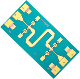
| Frequency Range(GHz) | Insertion loss (dB) | Clipping level (dBm) | Max. input power(dBm) |
| DC-20 | <0.3dB (full band) | 17 | 33(CW) |
| DC-6 | <0.1dB (full band) | 17 | 33(CW) |
| 2-18 | 0.4 | 19.5 | 40(CW) |
| DC-18 | ≤0.2dB | 17 | 33(CW) |
| 6-18 | 0.4 | 18 | 40(CW) |
| 5.3-5.9 | 0.9 | 16 | 200(CW) |
| 2.7-3.5 | 0.5 | 15 | 150(CW) |
| 1-6 | 0.4 | 15 | 200(Pulse) |
| 1-8 | 0.4 | 15.5 | 45(CW) |
| 8-12 | 0.7 | 18 | 47.8(Pulse) |
| 14-18 | 0.6 | 19 | 43(CW) |
High Power FET Switch
Features:
- Frequency range: DC-18GHz
- Switch type: SPST SPDT SP3T SP4T SP8T
- Anti-burn power up to 10W
- P-1>30dBm@20MHz
- Power supply: +5V or -5V, no high voltage required
| (GHz) | Insertion loss (dB) | Isolati on (dB) | Return loss (dB) | P-1 (dBm) | Switching time (ns) | Supply voltage (V) | Control voltage (V) | |
| SP2T | DC-22 | 1.3@20G | 38 | 20/20 | ≥30dBm @0.02~20GHz | 150 | +5 | 0/+3.3 |
| SP2T | DC-18 | 2.6@18G | 37 | 18/18 | ≥35Bm from 0.1GHz~18GHz | 180 | +5 | 0/+3.3 |
| SP2T | DC-18 | 1.5dB@18G | 47 | 15/16 | ≥40dBm from 0.5GHz~18GHz | 300 | — | 0/-5 |
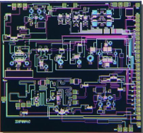
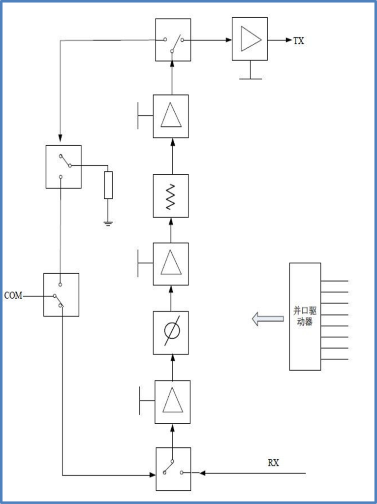
Gallium arsenide single channel amplitude and phase multi-function
Features:
- •broadband
- •Integrated logic control
- •Working frequency 7-13G
- •Customizable
| Electrical parameters(Ta=+25°C) | ||||
| parameter | Min | Typical value | Max | unit |
| Frequency Range | 7~13 | GHz | ||
| Emit Gain_TX | — | 17.5 | — | dB |
| Transmit gain flatness | — | ±1.8 | — | dB |
| Transmit P-1_TX | — | 19 | — | dBm |
| Transmit Psat_TX | — | 20.5 | — | dBm |
| Receive Gain_RX | — | 10.5 | — | dB |
| Receive gain flatness | — | ±1.3 | — | dB |
| Receive P-1 | — | 11.5 | — | dBm |
| Receive Psat | 13 | dBm | ||
| Receive noise figure | — | 8.5 | — | dB |
| Phase shift error (RMS) | — | 2.6 | — | Deg |
| Phase shift amplitude change | — | ±1.5 | — | dB |
| Attenuation error (RMS) | — | 0.4 | — | dB |
| Attenuation additional phase shift | — | ±6.5 | — | Deg |
| Port standing wave ratio | — | 1.5 | — | — |
| Transceiver switching time | — | <100 | — | ns |
Mixing multi-function chip
Features:
- Broadband
- Integrated local oscillator driver
- Integrated IF filter
- Customizable
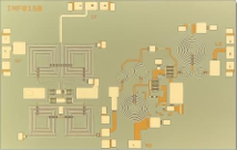
| RF/LO Frequency Range(GHz) | IF Frequency Range(GHz) | frequency conversion loss(dB) | LO-RF Isolation(dB) | Local vibration loss input power(dBm) | Voltage and current(V/mA) |
| 1-12 | DC-2 | 9 | 43 | 0~2 | 5/60 |
| 2-6 | DC-2.5 | 7.5 | 30 | 0~2 | 5/60 |
| 2-8 | DC-3 | 8 | 27 | 0~2 | 5/60 |
| 3-12 | DC-4 | 10 | 48 | 0~2 | 5/55 |
| 4-8 | DC-4 | 8 | 29 | 0~2 | 5/55 |
| 5-14 | DC-5 | 8 | 31 | 0~2 | 5/65 |
| 6-18 | DC-6 | 8 | 24 | 0~2 | 5/60 |
| 7-13 | DC-6.5 | 8 | 17 | 0-2 | 5/60 |
| 10-20 | DC-9 | 8 | 36 | 0~2 | 5/60 |
Transceiver multi-function chip
Features:
- •broadband
- •low noise
- •low cost
- •customizable
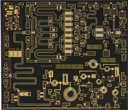
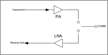
| frequency scope (GHz) | receive/tran smit Gain(dB) | Gain flatness (dB) | noise coefficient (dB) | Psat (dBm) | efficiency (%) | powered by (V/mA) |
| 8-10 | 28/27.5 | ±0.7 /±1.5 | 2.4 | 30.5 | 31 | +5V |
| 14-18 | 24.5/20.5 | ±0.5 /±0.4 | 2.6 | 24.5 | 32 | +5V |
| 14-18 | 24/26 | ±0.7 /±0.5 | 3.0 | 30.5 | 27 | +5V |
| 32-38 | 11.5/17.5 | ±0.25 /±1.5 | 3.5 | 27.5 | 16 | +5V |
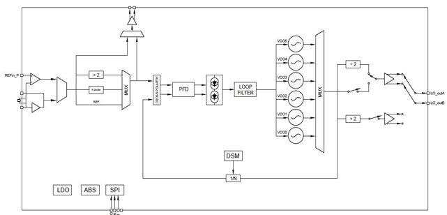
Silicon-based PLL frequency synthesis
Key features of PLL frequency synthesis chip:
- •Decimal Frequency Comprehensive
- •Supports external input reference clock, frequency range 40MHz~1000MHz.
- •It maintains an output frequency range of continuous LO frequency points between 2000MHz and 17000MHz.
- •Phase noise @16GHz: -85dBc/Hz @100Hz; -87dBc/Hz@1kHz; -93dBc/Hz@10KHz;
- -103dBc/Hz@100KHz; 120dBc/Hz@1MHz; 139dBc/Hz@10MHz.
- •Near-end spurious ≥45dBc.
- •Frequency hopping time is 500us.
- •clock jitter
- •65fs RMS jitter
- •Chip area 7x7mm
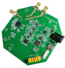
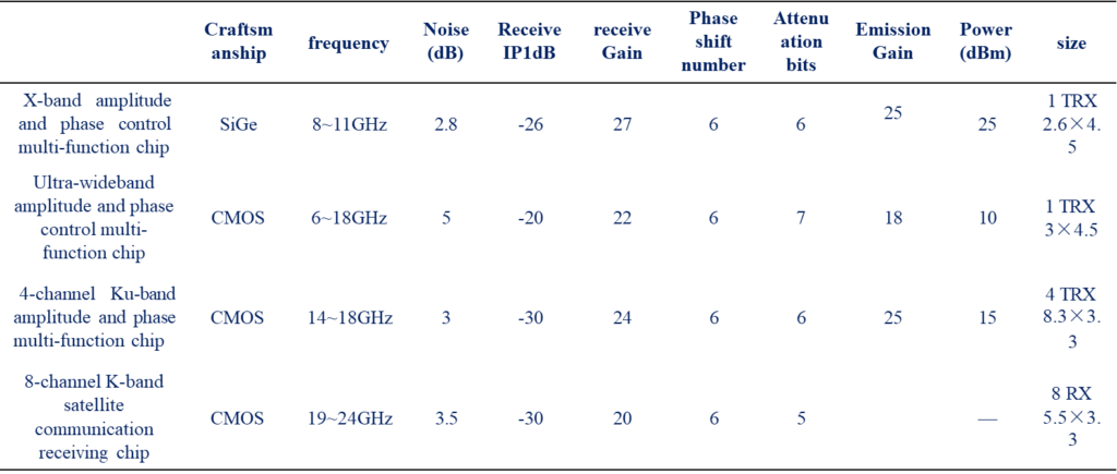
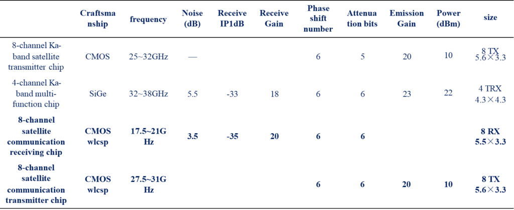
Silicon-based amplitude and phase control multi-function chip under development
SIP surface mount multi-function chip
Features:
- •Frequency to 12G
- •Functions can be matched as desired
- •Standard ceramic surface mount QFN packages 5×5, 7×7, 9×9, etc.
- •Low development costs
- •Fully automatic assembly and testing possible
- •High reliability

Millimeter wave packaging technology
Features:
- Frequency to 40G
- Standard ceramic surface mount 4x4mm, 5x5mm, 6x6mm packages
- Own production equipment, production technology and progress controllable
- Can be airtight
- National production, reliable supply chain
- Low cost
- Short proofing cycle


Low-cost, ceramic-to-metal packaged devices
Features:
- Frequency coverage to 4GHz
- High reliability
- Enterprise military standard production process
- Low cost
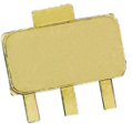
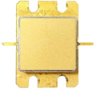
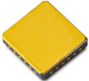
GaN internal matched power amplifier
Features:
- 960-1250MHz, 2.7~3.5GHz, 5~6GHz, 9.0-10.0GHz (pulse)
- Power level: 1500W (L-band), 400W (S-band), 300W (C-band), 200W (X-band)
- Efficiency: up to 70% or more
- 0.8-2GHz, 1-3GHz, 2-6GHz (continuous wave)
- Power level: 100W, 40W, 20W
- •Efficiency: 45%, 40%, 35%
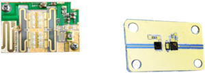
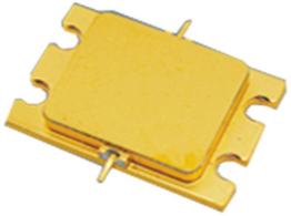
Ceramic filter
Features:
- Frequency coverage to 40GHz
- Low pass, high pass, band pass, band stop
- Customizable
- 100% tested on film
- Low cost
Useful info
Recommended installation:
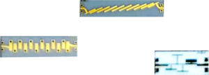
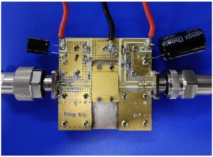
1. After tightening the tube casing with screws, the height between the tube casing pins and the printed board should be ≥0.1mm. The tube casing should be installed in the middle. The slot width should be ≥17.65mm. Ensure that the clearance between input and output end faces is >0.1mm, otherwise it may cause Pins come off. Can also be soldered.
2. It is recommended to use M2.0 screws, use 0.6N·m torque for assembly, and take anti-loosening measuressuch as spring washers, thread fasteners or nail cap dispensing.
3. When the device is working, the tube and shell temperature does not exceed 75°C.
Precautions:
1. This device is an internal matching device with an input and output impedance of 50Ω.
2. When powering up, please strictly follow the order of first negative pressure and then positive pressure;when powering on, add the gate voltage first, then add the leakage voltage; when powering off, first reduce the leakage voltage, then reduce the grid voltage.
3. Pay attention to heat dissipation during use. The lower the temperature of the tube and shell, the longer theservice life of the device.
4. During use, instruments, equipment, etc. should be well grounded; this product is an electrostatic sensitivedevice, so pay attention to anti-static when storing and using it.
Please select the power supply reasonably according to the specific modulation method and corresponding requirements

